Jumat, 14 Juli 2017

4440 AUDIO AMPLIFIER PCB DESIGN & MAKING

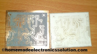
In a previous post I wrote how making printed circuit board in step by step. In this post I publish 4440 amplifier PCB making. This post is nearly same the previous post, but this post give you more info and guide you correctly to making the amplifier project. In amplifier if the PCB design is not correct, then the amplifier gives humming problem. This is happening when the ground is not properly connected & creates a ground loop. So remembered this problem I design the PCB that no humming are staying in amplified signal.

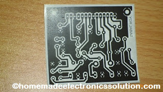
This is a PCB layout picture created by eagle cadsoftware. 

This is printed layout, when you print you must know how to print the layout. 


This picture is shown how looks after placing the layout in copper clad board. 


After etching, now you place the front of printed layout. 


After that rubbing & drilling the copper clad board looks like that. 


Now just place all the component & properly soldered. 


Finally, give a coating layer of varnish to protect the PCB track from corrosive material. Now this board looks like a professional PCB